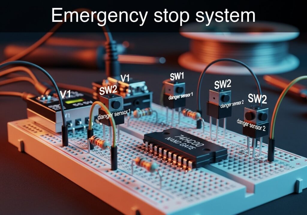
Level: Basic – Use the low-level output of a NAND gate to stop a process if two sensors detect danger simultaneously.
Objective and use case
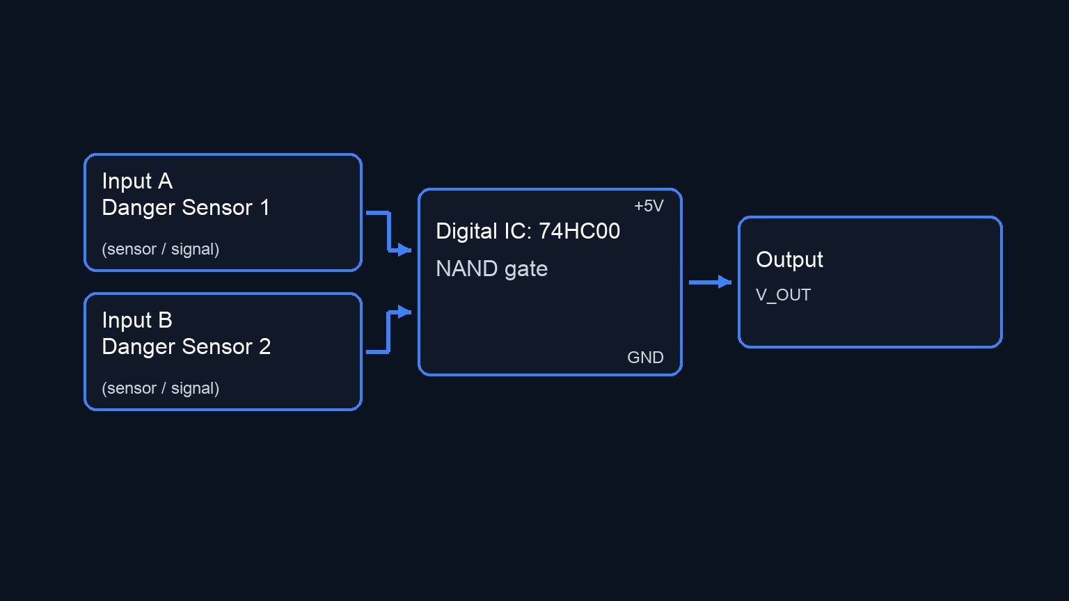
In this practical case, you will build a digital safety interlock circuit using a 74HC00 NAND gate. The system evaluates two independent danger sensors and triggers an active-low relay to halt a process only when both sensors detect a critical condition.
Why it is useful:
* Industrial safety: Halting heavy machinery if two separate safety guards are simultaneously bypassed or opened.
* Process control: Triggering an emergency shutdown in a chemical plant if both pressure and temperature exceed critical thresholds.
* Redundant validation: Preventing false alarms from shutting down a system by requiring two independent sensors to agree before taking action.
Expected outcome:
* When both sensors read a HIGH logic level (indicating danger), the NAND gate output will drop to a LOW logic level (~0 V).
* The 0 V signal will trigger an active-low relay module, engaging the emergency stop.
* If either or both sensors read a LOW logic level (safe condition), the NAND output remains HIGH (~5 V), keeping the relay inactive and the process running.
Target audience and level: Beginners in digital electronics and industrial logic control.
Materials
- V1: 5 V DC power supply
- SW1: SPST switch, function: danger sensor 1
- SW2: SPST switch, function: danger sensor 2
- R1: 10 kΩ resistor, function: pull-down for SW1
- R2: 10 kΩ resistor, function: pull-down for SW2
- U1: 74HC00 Quad 2-Input NAND gate IC
- RLY1: 5 V Active-low relay module, function: process emergency stop
Pin-out of the IC used
We will use the 74HC00 (Quad 2-Input NAND gate).
| Pin | Name | Logic function | Connection in this case |
|---|---|---|---|
| 1 | 1 A | Input 1 of Gate 1 | Node VA (from SW1) |
| 2 | 1B | Input 2 of Gate 1 | Node VB (from SW2) |
| 3 | 1Y | Output of Gate 1 | Node VOUT (to RLY1 IN) |
| 7 | GND | Ground | Node 0 |
| 14 | VCC | Power Supply | Node VCC |
Wiring guide
- V1: connects between node VCC and node 0 (GND).
- SW1: connects between node VCC and node VA.
- R1: connects between node VA and node 0.
- SW2: connects between node VCC and node VB.
- R2: connects between node VB and node 0.
- U1: Pin 14 connects to node VCC; Pin 7 connects to node 0.
- U1: Pin 1 connects to node VA.
- U1: Pin 2 connects to node VB.
- U1: Pin 3 connects to node VOUT.
- RLY1: VCC pin connects to node VCC, GND pin connects to node 0, and the signal/IN pin connects to node VOUT.
Conceptual block diagram
Schematic
POWER SUPPLY:
[ V1: 5 V DC Power Supply ] --(VCC)
                           --(GND)

SENSOR 1 INPUT PATH:
VCC --> [ SW1: Danger Sensor 1 ] --(Node VA)--> [ U1: 74HC00 NAND (Pin 1) ]
[ Node VA ] --> [ R1: 10 kΩ Pull-down ] --> GND

SENSOR 2 INPUT PATH:
VCC --> [ SW2: Danger Sensor 2 ] --(Node VB)--> [ U1: 74HC00 NAND (Pin 2) ]
[ Node VB ] --> [ R2: 10 kΩ Pull-down ] --> GND

LOGIC TO EMERGENCY STOP PATH:
[ U1: 74HC00 NAND (Pin 3) ] --(Node VOUT)--> [ RLY1: Relay Module (IN) ]

IC & MODULE POWER CONNECTIONS:
VCC --> [ U1: 74HC00 NAND (Pin 14) ]
GND <-- [ U1: 74HC00 NAND (Pin 7) ]

VCC --> [ RLY1: Relay Module (VCC) ]
GND <-- [ RLY1: Relay Module (GND) ]
Truth table
Note: The relay module in this case is active-low, meaning it triggers the emergency stop when it receives a 0.
| SW1 (Node VA) | SW2 (Node VB) | VOUT (NAND Output) | Relay State (Active-Low) | Process Status |
|---|---|---|---|---|
| 0 (Safe) | 0 (Safe) | 1 (HIGH) | OFF | Running |
| 0 (Safe) | 1 (Danger) | 1 (HIGH) | OFF | Running |
| 1 (Danger) | 0 (Safe) | 1 (HIGH) | OFF | Running |
| 1 (Danger) | 1 (Danger) | 0 (LOW) | ON (Triggered) | STOPPED |
Measurements and tests
- Input Logic States: Using a digital multimeter, measure the DC voltage at nodes VA and VB with respect to node 0. Verify they read ~0 V when the switches are open, and ~5 V when closed.
- Output Voltage Level: Measure node VOUT. Confirm it sits near 5 V during normal operation (when one or zero switches are closed).
- System Activation: Close both SW1 and SW2 simultaneously. Measure node VOUT to ensure it drops to ~0 V.
- Relay Actuation: Listen for the audible «click» of the relay (or observe its onboard indicator LED) precisely when VOUT drops to 0 V, confirming the emergency stop command has been physically executed.
SPICE netlist and simulation
Reference SPICE Netlist (ngspice) — excerptFull SPICE netlist (ngspice)
* Practical case: Emergency stop system
.width out=256

* Main 5V DC power supply
V1 VCC 0 DC 5

* SW1 (Danger sensor 1) and its pull-down resistor
S1 VCC VA ctrl1 0 sw_mod
Vctrl1 ctrl1 0 PULSE(0 5 0 1u 1u 50u 100u)
R1 VA 0 10k

* SW2 (Danger sensor 2) and its pull-down resistor
S2 VCC VB ctrl2 0 sw_mod
Vctrl2 ctrl2 0 PULSE(0 5 0 1u 1u 100u 200u)
R2 VB 0 10k

* U1: 74HC00 Quad 2-Input NAND gate IC (Using pins 1, 2, 3, 7, 14)
XU1 VA VB VOUT VCC 0 NAND_74HC00

* RLY1: 5V Active-low relay module
* ... (truncated in public view) ...
Copy this content into a .cir file and run with ngspice.
* Practical case: Emergency stop system
.width out=256

* Main 5V DC power supply
V1 VCC 0 DC 5

* SW1 (Danger sensor 1) and its pull-down resistor
S1 VCC VA ctrl1 0 sw_mod
Vctrl1 ctrl1 0 PULSE(0 5 0 1u 1u 50u 100u)
R1 VA 0 10k

* SW2 (Danger sensor 2) and its pull-down resistor
S2 VCC VB ctrl2 0 sw_mod
Vctrl2 ctrl2 0 PULSE(0 5 0 1u 1u 100u 200u)
R2 VB 0 10k

* U1: 74HC00 Quad 2-Input NAND gate IC (Using pins 1, 2, 3, 7, 14)
XU1 VA VB VOUT VCC 0 NAND_74HC00

* RLY1: 5V Active-low relay module
XRLY1 VOUT VCC 0 RELAY_MOD

* --- Subcircuits ---

.subckt NAND_74HC00 INA INB OUT VCC GND
* Behavioral NAND gate using continuous sigmoid functions for robust convergence
B1 OUT_int 0 V = 5 * (1 - (1/(1+exp(-20*(V(INA)-2.5)))) * (1/(1+exp(-20*(V(INB)-2.5)))))
R1 OUT_int OUT 100
C1 OUT 0 10p
.ends

.subckt RELAY_MOD IN VCC GND
* Simple resistive model for the relay module to satisfy load requirements
R_in IN GND 10k
R_vcc VCC GND 1k
.ends

* --- Models ---
.model sw_mod SW(Vt=2.5 Ron=0.1 Roff=100Meg)

* --- Analysis Directives ---
.tran 1u 300u
.print tran V(VA) V(VB)
.op
.end
Simulation Results (Transient Analysis)

Show raw data table (501 rows)
Index   time            v(va)           v(vb)
0	0.000000e+00	4.999500e-04	4.999500e-04
1	1.000000e-08	4.999500e-04	4.999500e-04
2	2.000000e-08	4.999500e-04	4.999500e-04
3	4.000000e-08	4.999500e-04	4.999500e-04
4	8.000000e-08	4.999500e-04	4.999500e-04
5	1.600000e-07	4.999500e-04	4.999500e-04
6	3.200000e-07	4.999500e-04	4.999500e-04
7	3.562500e-07	4.999500e-04	4.999500e-04
8	4.196875e-07	4.999500e-04	4.999500e-04
9	4.372461e-07	4.999500e-04	4.999500e-04
10	4.679736e-07	4.999500e-04	4.999500e-04
11	4.795524e-07	4.999500e-04	4.999500e-04
12	4.902290e-07	4.999500e-04	4.999500e-04
13	5.023412e-07	4.999950e+00	4.999950e+00
14	5.111724e-07	4.999950e+00	4.999950e+00
15	5.196372e-07	4.999950e+00	4.999950e+00
16	5.247062e-07	4.999950e+00	4.999950e+00
17	5.271308e-07	4.999950e+00	4.999950e+00
18	5.277087e-07	4.999950e+00	4.999950e+00
19	5.280739e-07	4.999950e+00	4.999950e+00
20	5.285244e-07	4.999950e+00	4.999950e+00
21	5.292184e-07	4.999950e+00	4.999950e+00
22	5.299733e-07	4.999950e+00	4.999950e+00
23	5.306602e-07	4.999950e+00	4.999950e+00
... (477 more rows) ...
Reference SPICE netlist (ngspice)
* Practical case: Emergency stop system
.width out=256

* Main 5V DC power supply
V1 VCC 0 DC 5

* SW1 (Danger sensor 1) and its pull-down resistor
S1 VCC VA ctrl1 0 sw_mod
Vctrl1 ctrl1 0 PULSE(0 5 0 1u 1u 50u 100u)
R1 VA 0 10k

* SW2 (Danger sensor 2) and its pull-down resistor
S2 VCC VB ctrl2 0 sw_mod
Vctrl2 ctrl2 0 PULSE(0 5 0 1u 1u 100u 200u)
R2 VB 0 10k

* U1: 74HC00 Quad 2-Input NAND gate IC (Using pins 1, 2, 3, 7, 14)
XU1 VA VB VOUT VCC 0 NAND_74HC00

* RLY1: 5V Active-low relay module
XRLY1 VOUT VCC 0 RELAY_MOD

* --- Subcircuits ---

.subckt NAND_74HC00 INA INB OUT VCC GND
* Behavioral NAND gate using continuous sigmoid functions for robust convergence
B1 OUT_int 0 V = 5 * (1 - (1/(1+exp(-20*(V(INA)-2.5)))) * (1/(1+exp(-20*(V(INB)-2.5)))))
R1 OUT_int OUT 100
C1 OUT 0 10p
.ends

.subckt RELAY_MOD IN VCC GND
* Simple resistive model for the relay module to satisfy load requirements
R_in IN GND 10k
R_vcc VCC GND 1k
.ends

* --- Models ---
.model sw_mod SW(Vt=2.5 Ron=0.1 Roff=100Meg)

* --- Analysis Directives ---
.tran 1u 300u
.print tran V(VA) V(VB)
.op
.end
Simulation Results (Transient Analysis)
Common mistakes and how to avoid them
- Floating inputs: Forgetting the pull-down resistors (R1 and R2). Without them, the logic gate inputs will float and pick up ambient noise, causing the relay to trigger randomly.
- Misunderstanding active-low logic: Expecting the relay to trigger when the output is 5 V. In this case, the NAND output drops to 0 V upon detecting mutual danger, which perfectly matches an active-low relay module. Ensure your relay module is truly active-low.
- Omitting IC power connections: Forgetting to wire pins 14 (VCC) and 7 (GND) of the 74HC00. The IC will not process logic without power, and may behave erratically if powered parasitically through its input pins.
Troubleshooting
- Symptom: The relay never clicks, even when both switches are closed.
- Cause: The 74HC00 output pin cannot sink enough current, or the relay module is active-high instead of active-low.
- Fix: Ensure you are using a relay module (with a built-in driver transistor) rather than a bare mechanical relay. Verify the module’s trigger logic (some have a jumper to select active-high vs. active-low).
- Symptom: The relay chatters rapidly or triggers randomly without human interaction.
- Cause: Floating inputs at node VA or VB.
- Fix: Double-check that R1 and R2 are properly seated in the breadboard and connected directly to GND (node 0).
- Symptom: The relay is always ON, and the process is permanently stopped.
- Cause: The NAND output is permanently stuck at 0 V. This can happen if both inputs are shorted to VCC, or if the logic gate is damaged.
- Fix: Measure VA and VB. If they are reading 0 V but VOUT is still 0 V, replace the 74HC00 IC.
Possible improvements and extensions
- Hardware debouncing: Add a 1 µF capacitor across each switch to prevent contact bounce from generating rapid, unintended logic transitions during the millisecond the switch is toggled.
- Visual status indicators: Connect an LED and a 330 Ω current-limiting resistor to node VOUT to provide a clear visual indicator on a control panel when the system is in a safe state (LED ON) versus an emergency state (LED OFF).
More Practical Cases on Prometeo.blog
Find this product and/or books on this topic on Amazon
As an Amazon Associate, I earn from qualifying purchases. If you buy through this link, you help keep this project running.
Quick Quiz

Telecommunications Electronics Engineer and Computer Engineer (official degrees in Spain).