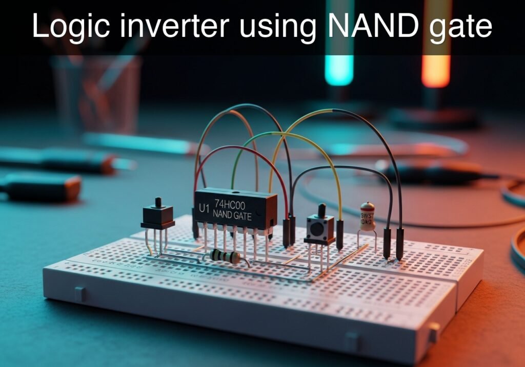
Level: Basic – Demonstrate the universality of the NAND gate by configuring it as a basic NOT gate.
Objective and use case
In this practical case, you will build a digital inverter (NOT gate) using a standard 74HC00 NAND gate by shorting its inputs together.
Understanding this configuration is highly useful for several reasons:
* BOM Optimization: It reduces the number of unique integrated circuits needed in a design; if you have spare NAND gates on a board, you do not need to add a dedicated NOT gate chip.
* Logic Universality: It practically proves that NAND gates are «universal,» meaning any logic function can be constructed using only NAND gates.
* Circuit Simplification: It helps streamline routing on printed circuit boards by repurposing nearby unused gates instead of running traces to a different IC.
Expected outcome:
* When the input switch provides a logic LOW (0 V) to the shorted inputs, the output will go HIGH (approx. 5 V), turning on the indicator LED.
* When the input switch provides a logic HIGH (5 V) to the shorted inputs, the output will go LOW (0 V), turning off the indicator LED.
* The circuit will perfectly replicate the behavior of a standard 74HC04 NOT gate.
Target audience: Electronics beginners learning fundamental Boolean algebra and digital hardware implementation.
Materials
- V1: 5 V DC supply
- U1: 74HC00 Quad 2-Input NAND Gate
- SW1: SPST toggle switch or push button, function: input state selector
- R1: 10 kΩ resistor, function: pull-down for node VA
- R2: 330 Ω resistor, function: current limiting for the output LED
- D1: Red LED, function: VOUT state indicator
Pin-out of the IC used
IC: 74HC00 (Quad 2-Input NAND gate)
| Pin | Name | Logic function | Connection in this case |
|---|---|---|---|
| 1 | 1 A | Input A of Gate 1 | Node VA (shorted to 1B) |
| 2 | 1B | Input B of Gate 1 | Node VA (shorted to 1 A) |
| 3 | 1Y | Output of Gate 1 | Node VOUT |
| 7 | GND | Ground | Node 0 |
| 14 | VCC | Positive Power Supply | Node VCC |
(Note: Pins 4, 5, 9, 10, 12, 13 are unused inputs in this specific exercise and should ideally be tied to Ground in a final physical circuit to prevent CMOS floating input issues).
Wiring guide
- V1: Connects between node VCC (+5 V) and node 0 (GND).
- U1 VCC/GND: Connect pin 14 to node VCC and pin 7 to node 0.
- SW1: Connects between node VCC and node VA.
- R1: Connects between node VA and node 0 (ensures a definitive LOW when the switch is open).
- U1 Inputs: Connect pin 1 (1 A) to node VA and connect pin 2 (1B) to node VA. This ties both inputs of the first NAND gate together.
- U1 Output: Pin 3 (1Y) provides the inverted signal and connects to node VOUT.
- R2: Connects between node VOUT and the anode of D1.
- D1: Connects the cathode to node 0.
Conceptual block diagram
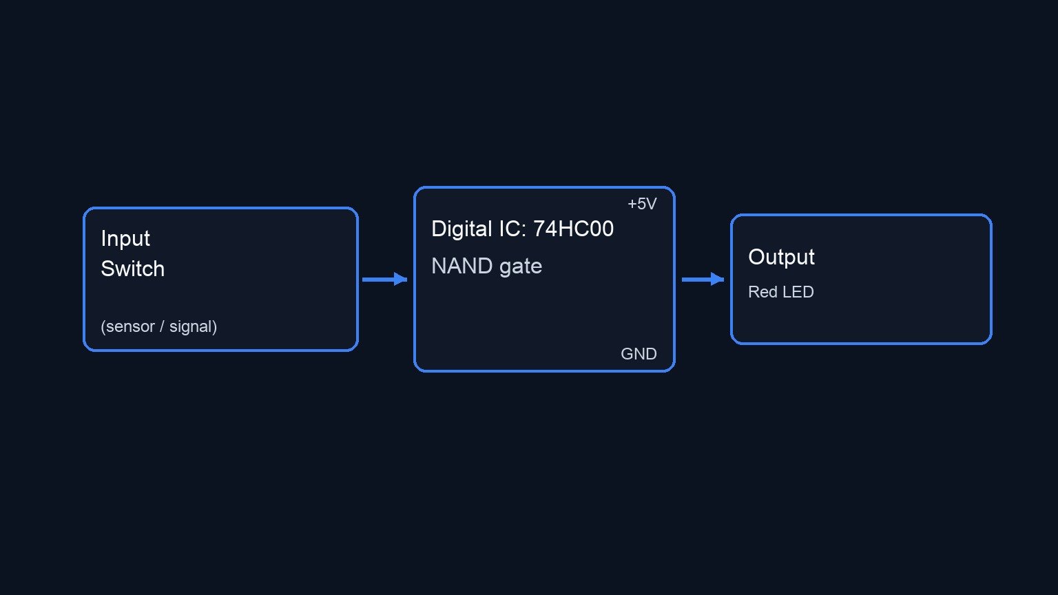
Schematic
VCC --> [ SW1: Switch ] --(Node VA)--> [ U1: 74HC00 NAND (Pins 1 & 2) ] --(VOUT)--> [ R2: 330 Ω ] --> [ D1: Red LED ] --> GND
                               |
                          [ R1: 10 kΩ ]
                               |
                              GND
Truth table
Input (VA) | Output (VOUT) | LED State (D1) |
|---|---|---|
| 0 (LOW) | 1 (HIGH) | ON |
| 1 (HIGH) | 0 (LOW) | OFF |
Measurements and tests
- Input Voltage Measurement: Use a multimeter to measure the voltage at node VA with respect to node 0. Verify that it reads ~0 V when SW1 is open, and ~5 V when SW1 is closed.
- Output Voltage Measurement: Move the multimeter probe to node VOUT. Confirm that it reads ~5 V when VA is 0 V, and reads ~0 V when VA is 5 V.
- Functional Verification: Toggle the switch multiple times. Ensure D1 behaves inversely to the physical action of the switch (e.g., if pressing the button sends a HIGH signal, the LED should turn off when pressed).
SPICE netlist and simulation
Reference SPICE Netlist (ngspice) — excerptFull SPICE netlist (ngspice)
* Practical case: Logic inverter using NAND gate

* Power Supply
V1 VCC 0 DC 5V

* Switch SW1 (VCC to VA)
* Modeled as a voltage-controlled switch to simulate user interaction
S_SW1 VCC VA SW_CTRL 0 sw_mod
.model sw_mod SW(vt=2.5 vh=0.2 ron=0.1 roff=100Meg)
V_SW_CTRL SW_CTRL 0 PULSE(0 5 10u 1u 1u 100u 200u)

* Pull-down resistor R1
R1 VA 0 10k

* U1: 74HC00 Quad 2-Input NAND Gate (using 1 gate)
* Pin 14: VCC, Pin 7: 0
* Pin 1: VA, Pin 2: VA, Pin 3: VOUT
XU1 VA VA VOUT VCC 0 NAND2_74HC00

* R2: Current limiting resistor
* ... (truncated in public view) ...
Copy this content into a .cir file and run with ngspice.
* Practical case: Logic inverter using NAND gate

* Power Supply
V1 VCC 0 DC 5V

* Switch SW1 (VCC to VA)
* Modeled as a voltage-controlled switch to simulate user interaction
S_SW1 VCC VA SW_CTRL 0 sw_mod
.model sw_mod SW(vt=2.5 vh=0.2 ron=0.1 roff=100Meg)
V_SW_CTRL SW_CTRL 0 PULSE(0 5 10u 1u 1u 100u 200u)

* Pull-down resistor R1
R1 VA 0 10k

* U1: 74HC00 Quad 2-Input NAND Gate (using 1 gate)
* Pin 14: VCC, Pin 7: 0
* Pin 1: VA, Pin 2: VA, Pin 3: VOUT
XU1 VA VA VOUT VCC 0 NAND2_74HC00

* R2: Current limiting resistor
R2 VOUT N1 330

* D1: Red LED
D1 N1 0 DLED

* Models
.model DLED D(IS=1e-15 N=1.8 RS=10)

* Subcircuit for NAND Gate
.subckt NAND2_74HC00 1A 1B 1Y VCC GND
RinA 1A GND 1G
RinB 1B GND 1G
Rvcc VCC GND 100Meg
B1 Y_int GND V = 5 * (1 - (1/(1+exp(-50*(V(1A)-2.5)))) * (1/(1+exp(-50*(V(1B)-2.5)))))
Rout Y_int 1Y 50
.ends

* Analysis
.tran 1u 600u
.print tran V(VA) V(VOUT) V(N1) I(V1)
.op
Simulation Results (Transient Analysis)

Show raw data table (704 rows)
Index   time            v(va)           v(vout)         v(n1)           v1#branch
0	0.000000e+00	4.999400e-04	4.537182e+00	1.482582e+00	-9.99950e-08
1	1.000000e-08	4.999400e-04	4.537182e+00	1.482580e+00	-9.99950e-08
2	2.000000e-08	4.999400e-04	4.537182e+00	1.482580e+00	-9.99950e-08
3	4.000000e-08	4.999400e-04	4.537182e+00	1.482580e+00	-9.99950e-08
4	8.000000e-08	4.999400e-04	4.537182e+00	1.482580e+00	-9.99950e-08
5	1.600000e-07	4.999400e-04	4.537182e+00	1.482580e+00	-9.99950e-08
6	3.200000e-07	4.999400e-04	4.537182e+00	1.482580e+00	-9.99950e-08
7	6.400000e-07	4.999400e-04	4.537182e+00	1.482580e+00	-9.99950e-08
8	1.280000e-06	4.999400e-04	4.537182e+00	1.482580e+00	-9.99950e-08
9	2.280000e-06	4.999400e-04	4.537182e+00	1.482580e+00	-9.99950e-08
10	3.280000e-06	4.999400e-04	4.537182e+00	1.482580e+00	-9.99950e-08
11	4.280000e-06	4.999400e-04	4.537182e+00	1.482580e+00	-9.99950e-08
12	5.280000e-06	4.999400e-04	4.537182e+00	1.482580e+00	-9.99950e-08
13	6.280000e-06	4.999400e-04	4.537182e+00	1.482580e+00	-9.99950e-08
14	7.280000e-06	4.999400e-04	4.537182e+00	1.482580e+00	-9.99950e-08
15	8.280000e-06	4.999400e-04	4.537182e+00	1.482580e+00	-9.99950e-08
16	9.280000e-06	4.999400e-04	4.537182e+00	1.482580e+00	-9.99950e-08
17	1.000000e-05	4.999400e-04	4.537182e+00	1.482580e+00	-9.99950e-08
18	1.010000e-05	4.999400e-04	4.537182e+00	1.482580e+00	-9.99950e-08
19	1.030000e-05	4.999400e-04	4.537182e+00	1.482580e+00	-9.99950e-08
20	1.034750e-05	4.999400e-04	4.537182e+00	1.482580e+00	-9.99950e-08
21	1.043062e-05	4.999400e-04	4.537182e+00	1.482580e+00	-9.99950e-08
22	1.045363e-05	4.999400e-04	4.537182e+00	1.482580e+00	-9.99950e-08
23	1.049390e-05	4.999400e-04	4.537182e+00	1.482580e+00	-9.99950e-08
... (680 more rows) ...
Reference SPICE netlist (ngspice)
* Practical case: Logic inverter using NAND gate

* Power Supply
V1 VCC 0 DC 5V

* Switch SW1 (VCC to VA)
* Modeled as a voltage-controlled switch to simulate user interaction
S_SW1 VCC VA SW_CTRL 0 sw_mod
.model sw_mod SW(vt=2.5 vh=0.2 ron=0.1 roff=100Meg)
V_SW_CTRL SW_CTRL 0 PULSE(0 5 10u 1u 1u 100u 200u)

* Pull-down resistor R1
R1 VA 0 10k

* U1: 74HC00 Quad 2-Input NAND Gate (using 1 gate)
* Pin 14: VCC, Pin 7: 0
* Pin 1: VA, Pin 2: VA, Pin 3: VOUT
XU1 VA VA VOUT VCC 0 NAND2_74HC00

* R2: Current limiting resistor
R2 VOUT N1 330

* D1: Red LED
D1 N1 0 DLED

* Models
.model DLED D(IS=1e-15 N=1.8 RS=10)

* Subcircuit for NAND Gate
.subckt NAND2_74HC00 1A 1B 1Y VCC GND
RinA 1A GND 1G
RinB 1B GND 1G
Rvcc VCC GND 100Meg
B1 Y_int GND V = 5 * (1 - (1/(1+exp(-50*(V(1A)-2.5)))) * (1/(1+exp(-50*(V(1B)-2.5)))))
Rout Y_int 1Y 50
.ends

* Analysis
.tran 1u 600u
.print tran V(VA) V(VOUT) V(N1) I(V1)
.op
Simulation Results (Transient Analysis)
Common mistakes and how to avoid them
- Leaving CMOS inputs floating: The 74HC00 is a CMOS IC. If you fail to use the pull-down resistor R1, opening SW1 will leave inputs 1 A and 1B floating, leading to erratic output switching and high power consumption. Always use a pull-up or pull-down resistor.
- Forgetting the LED current limiting resistor: Connecting D1 directly between VOUT and 0 without R2 will draw excessive current, potentially destroying both the LED and the output stage of the 74HC00 IC.
- Incorrectly shorting inputs: Mistakenly shorting an input to an output (e.g., bridging pins 2 and 3 instead of 1 and 2) will create a feedback loop or logic contention, preventing the circuit from functioning.
Troubleshooting
- Symptom: The LED never turns on.
- Cause: The LED (D1) might be inserted backwards, or the IC is unpowered.
- Fix: Check the polarity of the LED (anode to R2, cathode to 0). Measure the voltage between pins 14 and 7 to confirm the IC is receiving 5 V.
- Symptom: The LED is always on, regardless of the switch position.
- Cause: The switch is miswired, or the pull-up/pull-down configuration is incorrect (e.g., node VA is stuck LOW).
- Fix: Verify that SW1 applies 5 V to node VA when activated. Check R1 for a solid connection to Ground.
- Symptom: The IC becomes extremely hot.
- Cause: Power supply is reversed or there is a dead short at the output.
- Fix: Immediately disconnect power. Verify that pin 14 goes to VCC and pin 7 goes to 0. Ensure R2 is present in the output path.
Possible improvements and extensions
- Add an Input Indicator: Connect a second LED and resistor directly to node VA. This allows you to visually compare the input state and output state side-by-side (when one LED is ON, the other will be OFF).
- Build an AND Gate: Cascade this newly built inverter into a second NAND gate. Connect the output of a standard NAND gate to the shorted inputs of your NAND-based NOT gate to create a functional AND gate, further demonstrating universal logic.
More Practical Cases on Prometeo.blog
Find this product and/or books on this topic on Amazon
As an Amazon Associate, I earn from qualifying purchases. If you buy through this link, you help keep this project running.
Quick Quiz

Telecommunications Electronics Engineer and Computer Engineer (official degrees in Spain).