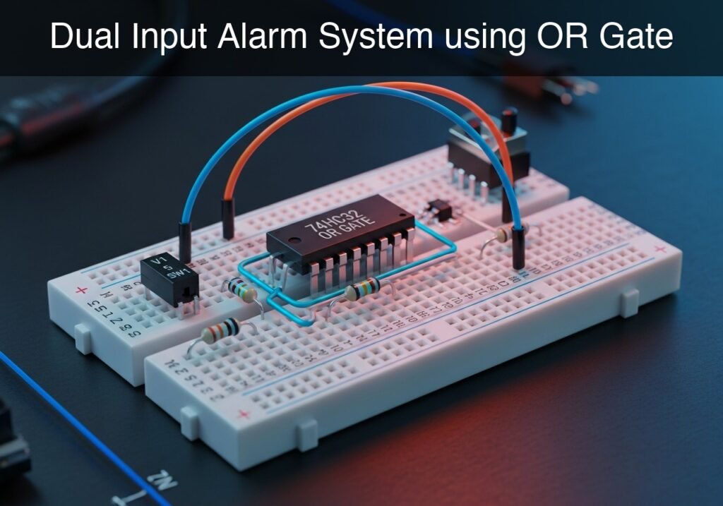
Level: Basic – Build an alert system that activates a warning LED when either a local or remote signal is triggered.
Objective and use case
In this practical case, you will build a digital alarm indicator utilizing a 74HC32 logic OR gate. The circuit combines two independent input signals (representing a local sensor and a remote sensor) so that if either one or both are activated, the output will drive an alert LED.
Why this circuit is useful:
* Security systems: A single alarm panel can monitor both a front door and a back door.
* Industrial safety: A machine can be halted by either a local emergency stop button or a remote operator console.
* Environmental monitoring: A system can trigger a unified warning if either a smoke detector or a heat sensor detects an anomaly.
Expected outcome:
* With both switches open (0 V at inputs), the output is 0 V and the LED is off.
* Closing the local switch yields 5 V at the first input, forcing the output to 5 V and turning on the LED.
* Closing the remote switch yields 5 V at the second input, forcing the output to 5 V and turning on the LED.
* Closing both switches simultaneously yields 5 V at both inputs, maintaining the 5 V output and keeping the LED illuminated.
Target audience and level: Beginners and hobbyists learning basic digital logic concepts.
Materials
- U1: 74HC32 quad 2-input OR gate, function: logic control
- V1: 5 V DC supply, function: power source
- SW1: SPST switch, function: local alarm trigger
- SW2: SPST switch, function: remote alarm trigger
- R1: 10 kΩ resistor, function: pull-down for VA
- R2: 10 kΩ resistor, function: pull-down for VB
- R3: 330 Ω resistor, function: LED current limiting
- D1: red LED, function: alarm indicator
Pin-out of the IC used
74HC32 (Quad 2-input OR gate)
| Pin | Name | Logic function | Connection in this case |
|---|---|---|---|
| 1 | 1 A | Input 1 for Gate 1 | Connects to node VA (from SW1) |
| 2 | 1B | Input 2 for Gate 1 | Connects to node VB (from SW2) |
| 3 | 1Y | Output of Gate 1 | Connects to node VOUT |
| 7 | GND | Ground / 0 V reference | Connects to node 0 |
| 14 | VCC | Positive supply voltage | Connects to node VCC |
(Note: Pins 4, 5, 6, 8, 9, 10, 11, 12, and 13 belong to the other three unused OR gates in the package and should ideally have their inputs tied to ground in a permanent design, though they are left out of this primary signal path for simplicity).
Wiring guide
- V1: Positive terminal connects to node VCC, negative terminal connects to node 0.
- SW1: Connects between node VCC and node VA.
- SW2: Connects between node VCC and node VB.
- R1: Connects between node VA and node 0.
- R2: Connects between node VB and node 0.
- U1: Pin 14 connects to node VCC, Pin 7 connects to node 0. Pin 1 connects to node VA, Pin 2 connects to node VB, Pin 3 connects to node VOUT.
- R3: Connects between node VOUT and node VLED.
- D1: Anode connects to node VLED, cathode connects to node 0.
Conceptual block diagram
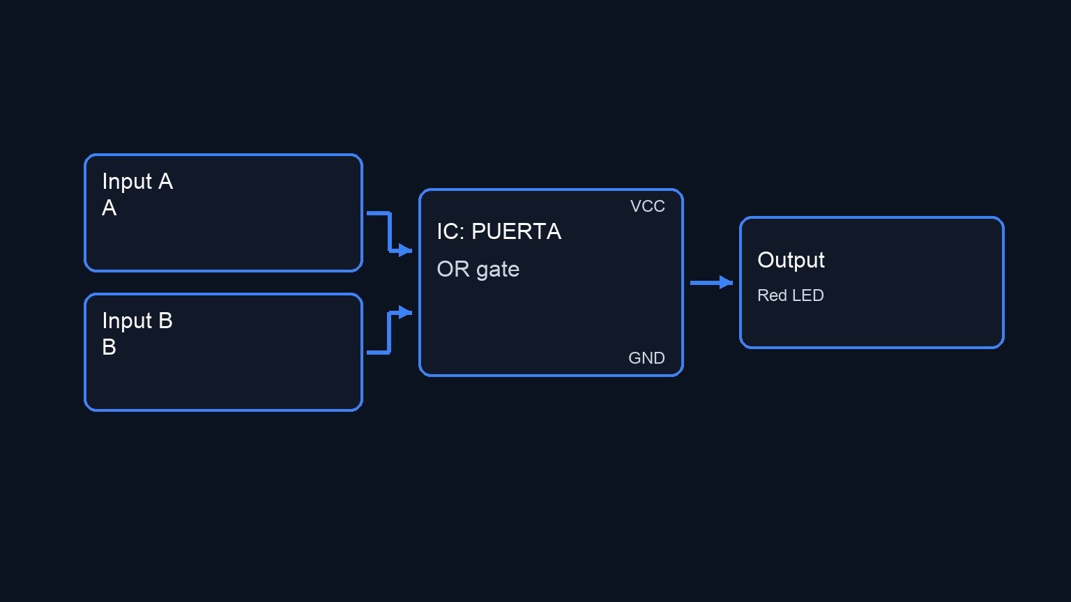
Schematic
VCC --> [ SW1: Local Alarm ] --(VA)-->+---------------------------------> [           ]
                                      |                                   [ U1: Pin 1 ]
                                      +--> [ R1: 10 kΩ Pull-down ] --> GND [           ]
                                                                          [  74HC32   ] --(VOUT)--> [ R3: 330 Ω ] --(VLED)--> [ D1: Red LED ] --> GND
VCC --> [ SW2: Remote Alarm] --(VB)-->+---------------------------------> [  OR Gate  ]
                                      |                                   [           ]
                                      +--> [ R2: 10 kΩ Pull-down ] --> GND [ U1: Pin 2 ]
                                                                          [           ]
Truth table
| Local Signal (VA) | Remote Signal (VB) | Output (VOUT) | Alarm LED (D1) |
|---|---|---|---|
| 0 (Low) | 0 (Low) | 0 (Low) | OFF |
| 0 (Low) | 1 (High) | 1 (High) | ON |
| 1 (High) | 0 (Low) | 1 (High) | ON |
| 1 (High) | 1 (High) | 1 (High) | ON |
Measurements and tests
- Input Verification: Using a digital multimeter (DMM) referenced to node 0, measure the voltage at nodes VA and VB. Verify that they read approximately 0 V when the respective switch is open, and 5 V when closed.
- Output Verification: Measure the voltage at node VOUT. Confirm that it reads 0 V only when both VA and VB are at 0 V. If either or both inputs are at 5 V, VOUT must measure close to 5 V.
- Visual Confirmation: Toggle SW1 and SW2 through all four possible combinations as listed in the truth table and confirm D1 behaves accordingly.
- Current Measurement (Optional): Place your DMM in series with R3 to measure the LED forward current. It should be approximately 8-10 mA depending on the LED’s forward voltage drop.
SPICE netlist and simulation
Reference SPICE Netlist (ngspice) — excerptFull SPICE netlist (ngspice)
* Dual Input Alarm System using OR Gate
.width out=256

* Power Supply
V1 VCC 0 DC 5

* Local Alarm Trigger (SW1)
* Modeled as a voltage-controlled switch driven by a pulse to simulate user interaction
SW1 VCC VA ctrl1 0 mySW
Vctrl1 ctrl1 0 PULSE(0 5 0 1u 1u 50u 100u)

* Remote Alarm Trigger (SW2)
* Modeled as a voltage-controlled switch driven by a pulse to simulate user interaction
SW2 VCC VB ctrl2 0 mySW
Vctrl2 ctrl2 0 PULSE(0 5 0 1u 1u 100u 200u)

* Switch Model
.model mySW SW(Ron=1 Roff=100Meg Vt=2.5)

* Pull-down resistors
* ... (truncated in public view) ...
Copy this content into a .cir file and run with ngspice.
* Dual Input Alarm System using OR Gate
.width out=256

* Power Supply
V1 VCC 0 DC 5

* Local Alarm Trigger (SW1)
* Modeled as a voltage-controlled switch driven by a pulse to simulate user interaction
SW1 VCC VA ctrl1 0 mySW
Vctrl1 ctrl1 0 PULSE(0 5 0 1u 1u 50u 100u)

* Remote Alarm Trigger (SW2)
* Modeled as a voltage-controlled switch driven by a pulse to simulate user interaction
SW2 VCC VB ctrl2 0 mySW
Vctrl2 ctrl2 0 PULSE(0 5 0 1u 1u 100u 200u)

* Switch Model
.model mySW SW(Ron=1 Roff=100Meg Vt=2.5)

* Pull-down resistors
R1 VA 0 10k
R2 VB 0 10k

* 74HC32 Quad 2-input OR gate (using 1 gate)
XU1 VA VB VOUT 0 VCC U_74HC32_OR

* Robust Subcircuit for 74HC32 OR Gate using continuous math functions
.subckt U_74HC32_OR P1 P2 P3 P7 P14
B1 P3 P7 V = V(P14,P7) * (1 - (1 / (1 + exp(50*(V(P1,P7)-V(P14,P7)/2)))) * (1 / (1 + exp(50*(V(P2,P7)-V(P14,P7)/2)))))
.ends

* Output Indicator
R3 VOUT VLED 330
D1 VLED 0 DLED
.model DLED D(IS=1e-15 N=1.8 RS=10)

* Analysis Commands
.tran 1u 300u
.print tran V(VA) V(VB) V(VOUT) V(VLED)
.op
Simulation Results (Transient Analysis)

Show raw data table (412 rows)
Index   time            v(va)           v(vb)           v(vout)         v(vled)
0	0.000000e+00	4.999500e-04	4.999500e-04	2.767481e-68	5.488664e-30
1	1.000000e-08	4.999500e-04	4.999500e-04	2.767481e-68	4.008316e-41
2	2.000000e-08	4.999500e-04	4.999500e-04	2.767481e-68	-4.00832e-41
3	4.000000e-08	4.999500e-04	4.999500e-04	2.767481e-68	-1.46362e-51
4	8.000000e-08	4.999500e-04	4.999500e-04	2.767481e-68	5.854466e-52
5	1.600000e-07	4.999500e-04	4.999500e-04	2.767481e-68	3.420369e-62
6	3.200000e-07	4.999500e-04	4.999500e-04	2.767481e-68	-8.55089e-63
7	3.562500e-07	4.999500e-04	4.999500e-04	2.767481e-68	2.767467e-68
8	4.196875e-07	4.999500e-04	4.999500e-04	2.767481e-68	2.767492e-68
9	4.372461e-07	4.999500e-04	4.999500e-04	2.767481e-68	2.767481e-68
10	4.679736e-07	4.999500e-04	4.999500e-04	2.767481e-68	2.767481e-68
11	5.019934e-07	4.999500e+00	4.999500e+00	5.000000e+00	1.503225e+00
12	5.700330e-07	4.999500e+00	4.999500e+00	5.000000e+00	1.502641e+00
13	7.061121e-07	4.999500e+00	4.999500e+00	5.000000e+00	1.502321e+00
14	9.782703e-07	4.999500e+00	4.999500e+00	5.000000e+00	1.502318e+00
15	1.000000e-06	4.999500e+00	4.999500e+00	5.000000e+00	1.502314e+00
16	1.043459e-06	4.999500e+00	4.999500e+00	5.000000e+00	1.502314e+00
17	1.130378e-06	4.999500e+00	4.999500e+00	5.000000e+00	1.502314e+00
18	1.304216e-06	4.999500e+00	4.999500e+00	5.000000e+00	1.502314e+00
19	1.651892e-06	4.999500e+00	4.999500e+00	5.000000e+00	1.502314e+00
20	2.347244e-06	4.999500e+00	4.999500e+00	5.000000e+00	1.502314e+00
21	3.347244e-06	4.999500e+00	4.999500e+00	5.000000e+00	1.502314e+00
22	4.347244e-06	4.999500e+00	4.999500e+00	5.000000e+00	1.502314e+00
23	5.347244e-06	4.999500e+00	4.999500e+00	5.000000e+00	1.502314e+00
... (388 more rows) ...
Reference SPICE netlist (ngspice)
* Dual Input Alarm System using OR Gate
.width out=256

* Power Supply
V1 VCC 0 DC 5

* Local Alarm Trigger (SW1)
* Modeled as a voltage-controlled switch driven by a pulse to simulate user interaction
SW1 VCC VA ctrl1 0 mySW
Vctrl1 ctrl1 0 PULSE(0 5 0 1u 1u 50u 100u)

* Remote Alarm Trigger (SW2)
* Modeled as a voltage-controlled switch driven by a pulse to simulate user interaction
SW2 VCC VB ctrl2 0 mySW
Vctrl2 ctrl2 0 PULSE(0 5 0 1u 1u 100u 200u)

* Switch Model
.model mySW SW(Ron=1 Roff=100Meg Vt=2.5)

* Pull-down resistors
R1 VA 0 10k
R2 VB 0 10k

* 74HC32 Quad 2-input OR gate (using 1 gate)
XU1 VA VB VOUT 0 VCC U_74HC32_OR

* Robust Subcircuit for 74HC32 OR Gate using continuous math functions
.subckt U_74HC32_OR P1 P2 P3 P7 P14
B1 P3 P7 V = V(P14,P7) * (1 - (1 / (1 + exp(50*(V(P1,P7)-V(P14,P7)/2)))) * (1 / (1 + exp(50*(V(P2,P7)-V(P14,P7)/2)))))
.ends

* Output Indicator
R3 VOUT VLED 330
D1 VLED 0 DLED
.model DLED D(IS=1e-15 N=1.8 RS=10)

* Analysis Commands
.tran 1u 300u
.print tran V(VA) V(VB) V(VOUT) V(VLED)
.op
Simulation Results (Transient Analysis)
Common mistakes and how to avoid them
- Floating inputs: Forgetting to connect the pull-down resistors (R1 and R2). Without them, when the switches are open, the 74HC32 inputs act like antennas and will cause the output to randomly toggle or oscillate. Always use pull-down resistors.
- Missing LED current limiting resistor: Connecting the LED directly from the output pin (node VOUT) to ground. This will draw excessive current, potentially burning out both the LED and the 74HC32 output stage. Always include R3.
- Forgetting IC power connections: Wiring the inputs and outputs but forgetting to supply VCC to pin 14 and GND to pin 7. The IC cannot function without its power rails connected.
Troubleshooting
- Symptom: The LED is always ON, regardless of switch positions.
- Cause: Inputs are permanently shorted to VCC, or switches are wired as «Normally Closed».
- Fix: Verify that the switches only bridge VCC to the inputs when actively pressed. Ensure nodes VA and VB measure 0 V when switches are released.
- Symptom: The LED never turns ON.
- Cause: LED D1 is inserted backwards (reversed polarity), or the IC is not powered.
- Fix: Check the orientation of D1 (anode to R3, cathode to ground). Measure pin 14 on U1 to guarantee it receives 5 V.
- Symptom: The LED flickers when you move your hand near the circuit.
- Cause: The inputs are floating. CMOS chips have highly sensitive inputs.
- Fix: Check the connections of R1 and R2. Ensure they securely tie nodes VA and VB to ground when the switches are open.
Possible improvements and extensions
- Audible alert integration: Add an active 5 V piezoelectric buzzer in parallel with the LED/resistor combination (connecting the buzzer’s positive lead to VOUT and the negative lead to node 0) to provide both a visual and audible alarm.
- Expand to a 3-input alarm: Utilize a second OR gate inside the same 74HC32 chip. Connect VOUT to Pin 4 (2 A), a third switch/pull-down assembly to Pin 5 (2B), and use Pin 6 (2Y) to drive the LED, creating a system that monitors three distinct zones.
More Practical Cases on Prometeo.blog
Find this product and/or books on this topic on Amazon
As an Amazon Associate, I earn from qualifying purchases. If you buy through this link, you help keep this project running.
Quick Quiz

Telecommunications Electronics Engineer and Computer Engineer (official degrees in Spain).