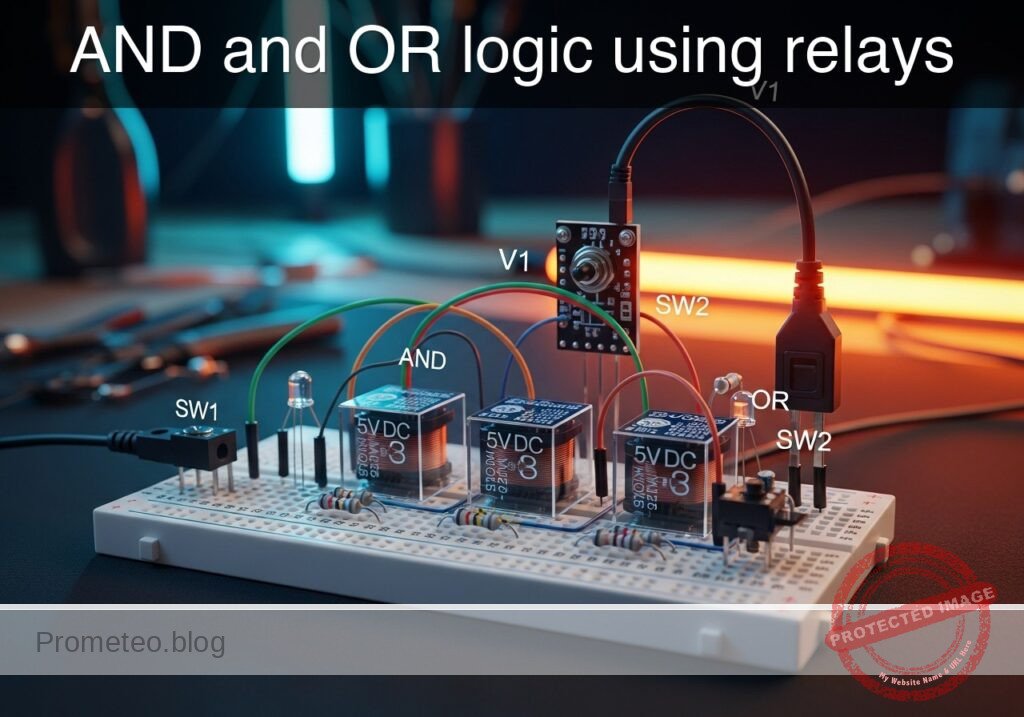
Level: Medium – Build basic logic gates by wiring the contacts of multiple relays in series and parallel.
Objective and use case
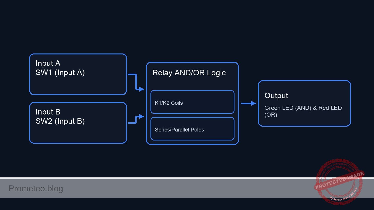
- What you will build: A circuit that utilizes two DPDT (Double Pole Double Throw) electro-mechanical relays to simultaneously demonstrate basic Boolean logic operations (AND and OR gates).
- Why it is useful:
- Forms the historical foundation of industrial automation and ladder logic programming.
- Demonstrates how to handle logic for high-voltage or high-current systems where standard silicon ICs are unsuitable.
- Provides complete electrical isolation between the control inputs (coils) and the logic outputs (contacts).
- Illustrates the fundamental fail-safe interlock principles used in heavy machinery and safety circuits.
- Expected outcome:
- The AND output (Green LED) will only illuminate when both relay coils are energized (series contacts).
- The OR output (Red LED) will illuminate when either relay coil is energized (parallel contacts).
- Successful measurement of control voltages confirming the activation of specific logic paths.
- Target audience and level: Intermediate electronics students exploring automated control systems and electromechanical switching.
Materials
- V1: 5 V DC supply, function: power for coils and logic
- SW1: SPST switch, function: Input A control
- SW2: SPST switch, function: Input B control
- K1: 5 V DPDT relay, function: Logic gate element A
- K2: 5 V DPDT relay, function: Logic gate element B
- D1: Green LED, function: AND logic output indicator
- D2: Red LED, function: OR logic output indicator
- D3: 1N4148 diode, function: K1 flyback protection
- D4: 1N4148 diode, function: K2 flyback protection
- R1: 330 Ω resistor, function: D1 current limiting
- R2: 330 Ω resistor, function: D2 current limiting
Wiring guide
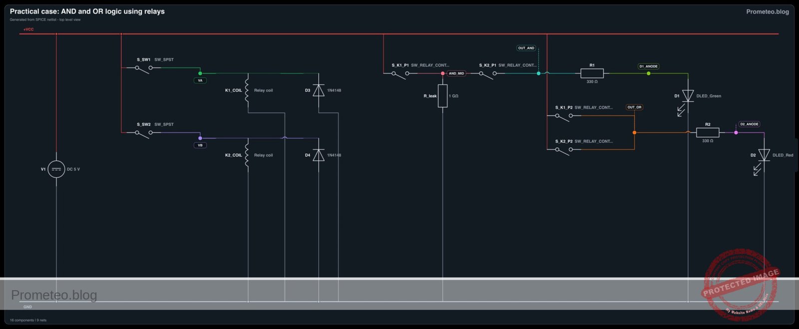
- V1 connects between VCC and 0.
- SW1 connects between VCC and node VA.
- SW2 connects between VCC and node VB.
- K1 coil connects between node VA and 0.
- K2 coil connects between node VB and 0.
- D3 cathode connects to node VA, anode connects to 0 (anti-parallel to K1 coil).
- D4 cathode connects to node VB, anode connects to 0 (anti-parallel to K2 coil).
- AND Logic (Series Wiring – Pole 1):
- K1 Pole 1 Common contact connects to VCC.
- K1 Pole 1 Normally Open (NO) contact connects to node AND_MID.
- K2 Pole 1 Common contact connects to node AND_MID.
- K2 Pole 1 Normally Open (NO) contact connects to node OUT_AND.
- OR Logic (Parallel Wiring – Pole 2):
- K1 Pole 2 Common contact connects to VCC.
- K1 Pole 2 Normally Open (NO) contact connects to node OUT_OR.
- K2 Pole 2 Common contact connects to VCC.
- K2 Pole 2 Normally Open (NO) contact connects to node OUT_OR.
- Outputs:
- R1 connects between OUT_AND and node D1_ANODE.
- D1 connects between D1_ANODE and 0 (cathode to ground).
- R2 connects between OUT_OR and node D2_ANODE.
- D2 connects between D2_ANODE and 0 (cathode to ground).
Conceptual block diagram
Schematic
[ CONTROL SECTION: RELAY COILS ]

VCC --> [ SW1 (Input A) ] --(VA)--> [ K1 Coil || D3(Rev) ] --> GND
                                          |
                                   (Magnetic Link)
                                          v
                                    (To K1 Poles)

VCC --> [ SW2 (Input B) ] --(VB)--> [ K2 Coil || D4(Rev) ] --> GND
                                          |
                                   (Magnetic Link)
                                          v
                                    (To K2 Poles)


[ AND LOGIC SECTION: SERIES WIRING (POLE 1) ]

VCC --> [ K1 Pole 1 (NO) ] --(AND_MID)--> [ K2 Pole 1 (NO) ] --(OUT_AND)--> [ R1 ] --(D1_ANODE)--> [ D1 (Green LED) ] --> GND


[ OR LOGIC SECTION: PARALLEL WIRING (POLE 2) ]

VCC --> [ K1 Pole 2 (NO) ] --(OUT_OR)--+
                                       |--> [ R2 ] --(D2_ANODE)--> [ D2 (Red LED) ] --> GND
VCC --> [ K2 Pole 2 (NO) ] --(OUT_OR)--+
Electrical diagram
Truth table
| Switch A (VA) | Switch B (VB) | K1 State | K2 State | AND Output (Green LED) | OR Output (Red LED) |
|---|---|---|---|---|---|
| OFF (0 V) | OFF (0 V) | Resting | Resting | OFF (0 V) | OFF (0 V) |
| OFF (0 V) | ON (5 V) | Resting | Energized | OFF (0 V) | ON (~5 V) |
| ON (5 V) | OFF (0 V) | Energized | Resting | OFF (0 V) | ON (~5 V) |
| ON (5 V) | ON (5 V) | Energized | Energized | ON (~5 V) | ON (~5 V) |
Measurements and tests
- Input Verification: Power on V1. Using a multimeter, measure the voltage at nodes VA and VB with respect to 0 (GND). Ensure it reads 0 V when the corresponding switch is open, and 5 V when closed.
- Mechanical Operation: Toggle SW1 and SW2 individually. You should hear a distinct mechanical «click» from K1 and K2, confirming coil activation.
- OR Gate Testing: Close SW1 only. Measure the voltage at OUT_OR (should be ~5 V) and ensure the Red LED lights up. Repeat this step for SW2 only.
- AND Gate Testing: Ensure both SW1 and SW2 are closed. Measure the voltage at OUT_AND (should be ~5 V) and confirm the Green LED lights up. If either switch is opened, the Green LED must turn off.
SPICE netlist and simulation
Reference SPICE Netlist (ngspice) — excerptFull SPICE netlist (ngspice)
* Practical case: AND and OR logic using relays
.width out=256

* Power Supply
V1 VCC 0 DC 5

* Input A Control (SW1)
* Modeled as a voltage-controlled switch toggled by a fast pulse source to simulate user input
S_SW1 VCC VA ctrl_A 0 switch_mod
V_ctrl_A ctrl_A 0 PULSE(0 5 0 1u 1u 100u 200u)

* Input B Control (SW2)
* Modeled as a voltage-controlled switch toggled by a fast pulse source
S_SW2 VCC VB ctrl_B 0 switch_mod
V_ctrl_B ctrl_B 0 PULSE(0 5 0 1u 1u 200u 400u)

* Relay K1 Coil and Flyback Diode
* Coil modeled as an RL series circuit
L_K1 VA K1_mid 1m
R_K1 K1_mid 0 100
* ... (truncated in public view) ...
Copy this content into a .cir file and run with ngspice.
* Practical case: AND and OR logic using relays
.width out=256

* Power Supply
V1 VCC 0 DC 5

* Input A Control (SW1)
* Modeled as a voltage-controlled switch toggled by a fast pulse source to simulate user input
S_SW1 VCC VA ctrl_A 0 switch_mod
V_ctrl_A ctrl_A 0 PULSE(0 5 0 1u 1u 100u 200u)

* Input B Control (SW2)
* Modeled as a voltage-controlled switch toggled by a fast pulse source
S_SW2 VCC VB ctrl_B 0 switch_mod
V_ctrl_B ctrl_B 0 PULSE(0 5 0 1u 1u 200u 400u)

* Relay K1 Coil and Flyback Diode
* Coil modeled as an RL series circuit
L_K1 VA K1_mid 1m
R_K1 K1_mid 0 100
D3 0 VA 1N4148

* Relay K2 Coil and Flyback Diode
L_K2 VB K2_mid 1m
R_K2 K2_mid 0 100
D4 0 VB 1N4148

* AND Logic (Series Wiring - Pole 1)
S_K1_P1 VCC AND_MID VA 0 relay_switch
S_K2_P1 AND_MID OUT_AND VB 0 relay_switch
* Anti-floating leak resistor for the midpoint of the series connection
R_leak AND_MID 0 1G

* OR Logic (Parallel Wiring - Pole 2)
S_K1_P2 VCC OUT_OR VA 0 relay_switch
S_K2_P2 VCC OUT_OR VB 0 relay_switch

* Outputs
R1 OUT_AND D1_ANODE 330
D1 D1_ANODE 0 DLED_Green

R2 OUT_OR D2_ANODE 330
D2 D2_ANODE 0 DLED_Red

* Models
.model switch_mod SW(vt=2.5 vh=0.5 ron=0.1 roff=100MEG)
.model relay_switch SW(vt=2.5 vh=0.5 ron=0.1 roff=100MEG)
.model 1N4148 D(IS=2.682n N=1.836 RS=0.5623 BV=100 IBV=100p CJO=4p M=0.333 VJ=0.5 TT=11.54n)
.model DLED_Green D(IS=1e-20 N=2.2 RS=5)
.model DLED_Red D(IS=1e-15 N=2.0 RS=5)

* Analysis
.tran 1u 500u
.print tran V(VA) V(VB) V(OUT_AND) V(OUT_OR) V(AND_MID) I(L_K1)
.op
.end
Simulation Results (Transient Analysis)

Analysis: The simulation results match the expected truth table for AND and OR logic. When both inputs are 5V, both outputs are near 5V. When only one input is 5V, only the OR output goes to 5V. The OFF state voltages are non-zero (around 1.6V and 0.9V) due to the finite off-resistance of the switch models, but these are below the LED forward voltages.
Show raw data table (5166 rows)
Index   time            v(va)           v(vb)           v(out_and)      v(out_or)       v(and_mid)      l_k1#branch
0	0.000000e+00	4.999967e-06	4.999967e-06	1.597015e+00	9.421253e-01	3.141436e+00	4.999967e-08
1	1.000000e-08	4.999967e-06	4.999967e-06	1.597015e+00	9.421253e-01	3.141436e+00	4.999967e-08
2	2.000000e-08	4.999967e-06	4.999967e-06	1.597015e+00	9.421253e-01	3.141436e+00	4.999967e-08
3	4.000000e-08	4.999967e-06	4.999967e-06	1.597015e+00	9.421253e-01	3.141436e+00	4.999967e-08
4	8.000000e-08	4.999967e-06	4.999967e-06	1.597015e+00	9.421253e-01	3.141436e+00	4.999967e-08
5	1.600000e-07	4.999967e-06	4.999967e-06	1.597015e+00	9.421253e-01	3.141436e+00	4.999967e-08
6	3.200000e-07	4.999967e-06	4.999967e-06	1.597015e+00	9.421253e-01	3.141436e+00	4.999967e-08
7	3.750000e-07	4.999967e-06	4.999967e-06	1.597015e+00	9.421253e-01	3.141436e+00	4.999967e-08
8	4.712500e-07	4.999967e-06	4.999967e-06	1.597015e+00	9.421253e-01	3.141436e+00	4.999967e-08
9	4.978906e-07	4.999967e-06	4.999967e-06	1.597015e+00	9.421253e-01	3.141436e+00	4.999967e-08
10	5.445117e-07	4.999967e-06	4.999967e-06	1.597015e+00	9.421253e-01	3.141436e+00	4.999967e-08
11	5.574158e-07	4.999967e-06	4.999967e-06	1.597015e+00	9.421253e-01	3.141436e+00	4.999967e-08
12	5.799979e-07	4.999967e-06	4.999967e-06	1.597015e+00	9.421253e-01	3.141436e+00	4.999967e-08
13	6.019875e-07	4.999887e+00	4.999887e+00	4.998416e+00	4.999485e+00	4.999208e+00	5.496234e-05
14	6.174611e-07	5.000094e+00	5.000094e+00	4.998416e+00	4.999485e+00	4.999208e+00	1.321856e-04
15	6.317917e-07	4.999872e+00	4.999872e+00	4.998416e+00	4.999485e+00	4.999208e+00	2.035976e-04
16	6.498539e-07	5.000078e+00	5.000078e+00	4.998416e+00	4.999485e+00	4.999208e+00	2.934595e-04
17	6.859784e-07	4.999845e+00	4.999845e+00	4.998416e+00	4.999485e+00	4.999208e+00	4.726966e-04
18	7.582273e-07	5.000025e+00	5.000025e+00	4.998416e+00	4.999485e+00	4.999208e+00	8.292335e-04
19	9.027252e-07	4.999739e+00	4.999739e+00	4.998416e+00	4.999485e+00	4.999208e+00	1.534627e-03
20	1.000000e-06	4.999907e+00	4.999907e+00	4.998416e+00	4.999485e+00	4.999208e+00	2.003774e-03
21	1.028900e-06	4.999786e+00	4.999786e+00	4.998416e+00	4.999485e+00	4.999208e+00	2.142075e-03
22	1.086699e-06	4.999758e+00	4.999758e+00	4.998416e+00	4.999485e+00	4.999208e+00	2.417880e-03
23	1.202297e-06	4.999704e+00	4.999704e+00	4.998416e+00	4.999485e+00	4.999208e+00	2.964729e-03
... (5142 more rows) ...
Reference SPICE netlist (ngspice)
* Practical case: AND and OR logic using relays
.width out=256

* Power Supply
V1 VCC 0 DC 5

* Input A Control (SW1)
* Modeled as a voltage-controlled switch toggled by a fast pulse source to simulate user input
S_SW1 VCC VA ctrl_A 0 switch_mod
V_ctrl_A ctrl_A 0 PULSE(0 5 0 1u 1u 100u 200u)

* Input B Control (SW2)
* Modeled as a voltage-controlled switch toggled by a fast pulse source
S_SW2 VCC VB ctrl_B 0 switch_mod
V_ctrl_B ctrl_B 0 PULSE(0 5 0 1u 1u 200u 400u)

* Relay K1 Coil and Flyback Diode
* Coil modeled as an RL series circuit
L_K1 VA K1_mid 1m
R_K1 K1_mid 0 100
D3 0 VA 1N4148

* Relay K2 Coil and Flyback Diode
L_K2 VB K2_mid 1m
R_K2 K2_mid 0 100
D4 0 VB 1N4148

* AND Logic (Series Wiring - Pole 1)
S_K1_P1 VCC AND_MID VA 0 relay_switch
S_K2_P1 AND_MID OUT_AND VB 0 relay_switch
* Anti-floating leak resistor for the midpoint of the series connection
R_leak AND_MID 0 1G

* OR Logic (Parallel Wiring - Pole 2)
S_K1_P2 VCC OUT_OR VA 0 relay_switch
S_K2_P2 VCC OUT_OR VB 0 relay_switch

* Outputs
R1 OUT_AND D1_ANODE 330
D1 D1_ANODE 0 DLED_Green

R2 OUT_OR D2_ANODE 330
D2 D2_ANODE 0 DLED_Red

* Models
.model switch_mod SW(vt=2.5 vh=0.5 ron=0.1 roff=100MEG)
.model relay_switch SW(vt=2.5 vh=0.5 ron=0.1 roff=100MEG)
.model 1N4148 D(IS=2.682n N=1.836 RS=0.5623 BV=100 IBV=100p CJO=4p M=0.333 VJ=0.5 TT=11.54n)
.model DLED_Green D(IS=1e-20 N=2.2 RS=5)
.model DLED_Red D(IS=1e-15 N=2.0 RS=5)

* Analysis
.tran 1u 500u
.print tran V(VA) V(VB) V(OUT_AND) V(OUT_OR) V(AND_MID) I(L_K1)
.op
.end
Simulation Results (Transient Analysis)
Analysis: The simulation results match the expected truth table for AND and OR logic. When both inputs are 5V, both outputs are near 5V. When only one input is 5V, only the OR output goes to 5V. The OFF state voltages are non-zero (around 1.6V and 0.9V) due to the finite off-resistance of the switch models, but these are below the LED forward voltages.
Common mistakes and how to avoid them
- Omitting flyback diodes: Failing to include D3 and D4 can cause high voltage spikes when the switches are opened, which can damage the switches or surrounding sensitive electronics. Always wire them in reverse-bias across the coils.
- Confusing NO and NC contacts: Accidentally wiring to the Normally Closed (NC) pin instead of the Normally Open (NO) pin will invert the logic, effectively creating NAND/NOR conditions instead of AND/OR. Double-check your relay’s datasheet or pinout.
- Insufficient power supply current: Relays consume significantly more current than digital ICs (often 50–100 mA per coil). Ensure your 5 V supply can comfortably deliver at least 300 mA to prevent voltage dips when both relays are energized.
Troubleshooting
- Symptom: Neither LED lights up under any switch combination, and no «clicks» are heard.
- Cause: Power supply V1 is disconnected, dead, or current-limited.
- Fix: Verify VCC and 0 connections to the main supply and check the supply limits.
- Symptom: Relays click when switches are pressed, but LEDs never turn on.
- Cause: The control side (coils) is working, but the logic side (contacts) is unpowered.
- Fix: Verify that VCC is properly routed to the Common pins of both poles on K1 and K2.
- Symptom: Power supply resets or dips severely when a switch is pressed.
- Cause: A flyback diode (D3 or D4) is installed backward, creating a direct short circuit to ground when the switch closes.
- Fix: Check diode orientation; the cathode (striped side) must face the positive incoming voltage (VA or VB).
- Symptom: The AND logic acts like an OR logic.
- Cause: The contacts for the AND gate were wired in parallel instead of series.
- Fix: Inspect the node AND_MID. VCC should strictly flow through K1 into K2, not directly to both.
Possible improvements and extensions
- Implement a NOT Gate (Inverter): Add a third relay or utilize an unused pole. Route VCC through its Normally Closed (NC) contact so that the output turns OFF when the relay is energized.
- Build an XOR (Exclusive OR) Circuit: Using both poles of two SPDT/DPDT relays, wire the NO contact of K1 to the NC contact of K2, and the NC contact of K1 to the NO contact of K2. This implements a 2-way lighting circuit logic using relays.
More Practical Cases on Prometeo.blog
Find this product and/or books on this topic on Amazon
As an Amazon Associate, I earn from qualifying purchases. If you buy through this link, you help keep this project running.
Quick Quiz

Carlos Núñez Zorrilla
Electronics & Computer Engineer
Telecommunications Electronics Engineer and Computer Engineer (official degrees in Spain).