Objective and use case
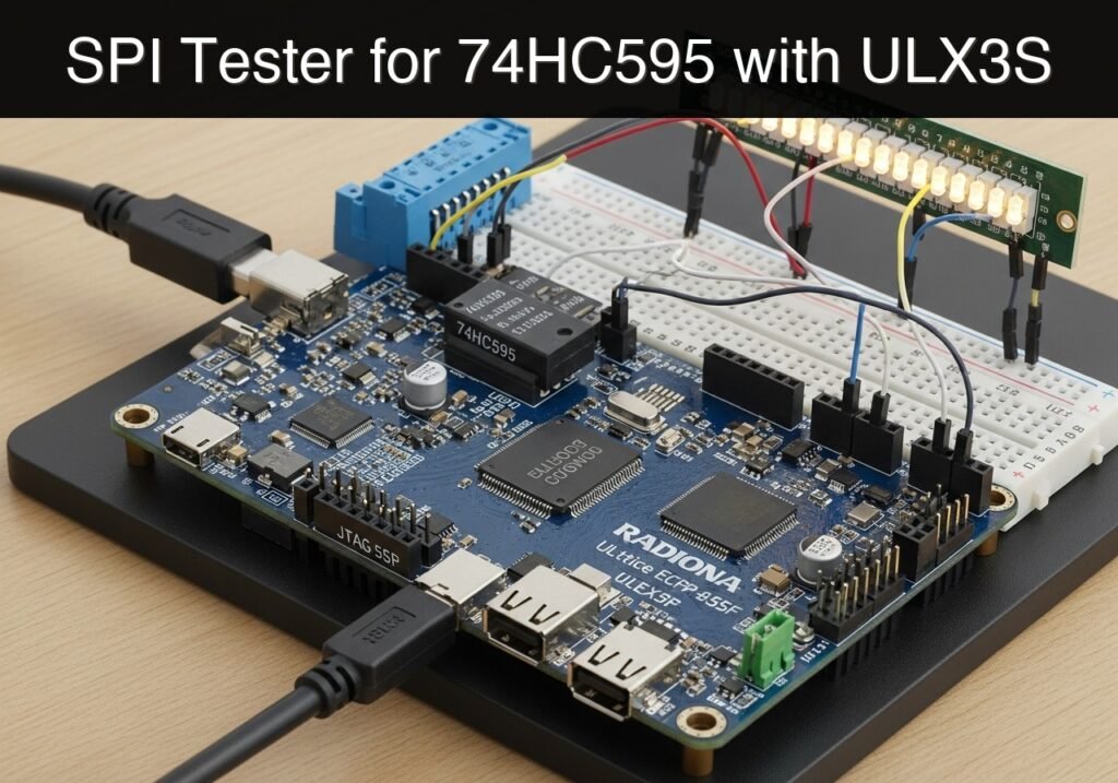
What you’ll build: A hardware-based SPI shift register output tester on the Radiona ULX3S that drives an external 74HC595 IC and LED bar. This dedicated testing tool generates reliable SPI test patterns to verify external component integrity and isolate physical hardware faults from firmware bugs.
Why it matters / Use cases
- PCB Assembly Validation: Test custom boards to ensure all 74HC595 pins are correctly soldered without shorts or bridges.
- Component Integrity Checking: Verify that a batch of shift register ICs is fully functional before soldering them into a final product.
- SPI Signal Debugging: Provide a continuous, predictable SPI master signal (MOSI, SCK, CS) at known frequencies (e.g., 1–10 MHz) to calibrate oscilloscopes or logic analyzers.
- Automated Burn-in: Run continuous alternating bit patterns on external LED matrix modules to test long-term hardware stability.
Expected outcome
- A verified, known-good SPI master bitstream running on the ULX3S FPGA with predictable timing.
- Visual confirmation of hardware integrity via an actively driven external LED bar graph displaying alternating test patterns.
- Clear isolation of faults between FPGA firmware, SPI protocol timing, and physical PCB hardware.
Audience: Hardware engineers, FPGA developers, and PCB designers; Level: Intermediate
Architecture/flow: The ULX3S FPGA generates a continuous SPI master signal (SCK, MOSI, CS) routed through GPIO pins to an external 74HC595 shift register, which decodes the serial data into a parallel output to drive the LED bar.
Educational validation note
Before publication, this case passed the Prometeo automated validation gate with status PASS. For this FPGA/ULX3S profile, the synthesizable Verilog blocks were checked with Yosys (read_verilog) and the Verilog design/test set was linted with Verilator. The validator also checked code-block structure, copy/paste-safe ASCII command options, unsupported stacks, and availability of the ULX3S/ECP5 toolchain (yosys, nextpnr-ecp5, ecppack, openFPGALoader).
Published validation evidence
- Automatic result: PASS.
- Parsed structure: 3 sections, 1 tables and 5 code blocks detected before publication.
- Checked code: 3 Verilog/Yosys-Verilator, 1 Bash/copy-paste checks.
- Supported catalog: the article text was checked against Prometeo’s validation-capable device profiles, and unsupported stacks block publication.
- Report findings: no blocking findings.
This validation confirms syntax and tool compatibility for the published code, but it does not replace physical testing on your exact ULX3S board revision, pin-constraint file and real wiring.
Educational safety note
This project is an educational prototype, not a certified product. Before powering the setup, verify the pinout of your exact ULX3S board revision, keep FPGA I/O signals at 3.3 V, never connect 5 V directly to I/O pins, disconnect power before changing wiring, and use suitable external supplies for loads, motors or servos while sharing ground only when the wiring requires it.
Prerequisites
- Basic understanding of digital logic (clocks, state machines, registers).
- Familiarity with the Serial Peripheral Interface (SPI) protocol (specifically MOSI, SCK, and Chip Select/Latch).
- A working installation of the open-source Lattice ECP5 FPGA toolchain: Yosys, nextpnr-ecp5, Project Trellis (ecppack), and openFPGALoader.
- Verilator installed for linting and simulation.
Materials
- FPGA Board: Radiona ULX3S (Lattice ECP5-85F variant).
- Shift Register: 1x 74HC595 8-bit shift register IC (DIP package for breadboarding).
- Display: 1x 10-segment LED bar graph (we will use 8 segments).
- Passive Components: 8x 330Ω resistors.
- Prototyping: 1x Breadboard and a set of male-to-male and male-to-female jumper wires.
Setup/Connection
The 74HC595 requires specific control pins to be tied to logic levels to operate correctly. The ULX3S operates at 3.3V logic, which is fully compatible with the 74HC595 VCC. Connect the components according to the table below.
| ULX3S Pin | ULX3S Port | 74HC595 Pin | Description |
|---|---|---|---|
| 3.3V | 3.3V | 16 (VCC) & 10 (SRCLR) | Power and active-low shift register clear (tied high) |
| GND | GND | 8 (GND) & 13 (OE) | Ground and active-low output enable (tied low) |
| B11 | gp[0] | 14 (SER) | SPI MOSI (Serial Data) |
| C11 | gp[1] | 11 (SRCLK) | SPI SCK (Serial Clock) |
| A10 | gp[2] | 12 (RCLK) | SPI Latch (Register Clock) |
For the outputs to the LED Bar:
1. Connect 74HC595 Pins 15, 1, 2, 3, 4, 5, 6, 7 (Q0 through Q7) to the anodes of the first 8 segments of the LED bar.
2. Connect the corresponding 8 cathodes of the LED bar to the Ground rail through 330Ω current-limiting resistors.
Validated Code
The project is divided into three synthesizable Verilog files, one testbench, and one physical constraints file. Keep them in the same working directory.
spi_master.v
This module handles the physical serialization of the 8-bit data. It waits for a start signal, shifts out the data MSB-first on the MOSI line, toggles the SCK line, and finally pulses the LATCH line.
Public preview of the validated file. The complete source is shown to members and in PDF/Print.
/* spi_master.v */
module spi_master (
    input wire clk,          // System clock
    input wire rst,          // Active high reset
    input wire start,        // Pulse high to start transmission
    input wire [7:0] data_in,// Data to transmit
    output reg mosi,         // Master Out Slave In
    output reg sck,          // Serial Clock
    output reg latch,        // Register Latch (RCLK)
    output reg busy          // High while transmitting
);

    reg [3:0] bit_cnt;
    reg [7:0] shift_reg;
    reg [2:0] state;

    localparam IDLE  = 3'd0;
    localparam LOAD  = 3'd1;
    localparam LOW   = 3'd2;
    localparam HIGH  = 3'd3;
    localparam LATCH = 3'd4;

    always @(posedge clk or posedge rst) begin
        if (rst) begin
            mosi <= 1'b0;
            sck <= 1'b0;
            latch <= 1'b0;
            busy <= 1'b0;
            bit_cnt <= 4'd0;
            shift_reg <= 8'd0;
            state <= IDLE;
        end else begin
            case (state)
                IDLE: begin
                    latch <= 1'b0;
                    sck <= 1'b0;
                    if (start) begin
                        shift_reg <= data_in;
                        busy <= 1'b1;
// .../* spi_master.v */
module spi_master (
input wire clk, // System clock
input wire rst, // Active high reset
input wire start, // Pulse high to start transmission
input wire [7:0] data_in,// Data to transmit
output reg mosi, // Master Out Slave In
output reg sck, // Serial Clock
output reg latch, // Register Latch (RCLK)
output reg busy // High while transmitting
);
reg [3:0] bit_cnt;
reg [7:0] shift_reg;
reg [2:0] state;
localparam IDLE = 3'd0;
localparam LOAD = 3'd1;
localparam LOW = 3'd2;
localparam HIGH = 3'd3;
localparam LATCH = 3'd4;
always @(posedge clk or posedge rst) begin
if (rst) begin
mosi <= 1'b0;
sck <= 1'b0;
latch <= 1'b0;
busy <= 1'b0;
bit_cnt <= 4'd0;
shift_reg <= 8'd0;
state <= IDLE;
end else begin
case (state)
IDLE: begin
latch <= 1'b0;
sck <= 1'b0;
if (start) begin
shift_reg <= data_in;
busy <= 1'b1;
                        bit_cnt <= 4'd8;
                        state <= LOAD;
                    end else begin
                        busy <= 1'b0;
                    end
                end

                LOAD: begin
                    mosi <= shift_reg[7];
                    shift_reg <= {shift_reg[6:0], 1'b0};
                    sck <= 1'b0;
                    state <= HIGH;
                end

                HIGH: begin
                    sck <= 1'b1;
                    bit_cnt <= bit_cnt - 4'd1;
                    state <= LOW;
                end

                LOW: begin
                    sck <= 1'b0;
                    if (bit_cnt == 4'd0) begin
                        state <= LATCH;
                    end else begin
                        state <= LOAD;
                    end
                end
LATCH: begin
latch <= 1'b1;
state <= IDLE;
end
default: state <= IDLE;
endcase
end
end
endmodule
tester_top.v
This is the top-level module. It divides the 25 MHz ULX3S clock to create an update tick for the patterns and a ~3 MHz clock for the SPI master (resulting in a ~1.5 MHz SCK). It also debounces the user button and cycles through four test patterns.
Public preview of the validated file. The complete source is shown to members and in PDF/Print.
/* tester_top.v */
module tester_top #(
    parameter TIMER_BITS = 24 // Can be reduced for simulation speed
)(
    input wire clk_25mhz,
    input wire [2:1] btn,
    output wire spi_mosi,
    output wire spi_sck,
    output wire spi_latch
);

    wire rst = btn[1];
    wire mode_btn = btn[2];

    // Clock dividers
    reg [TIMER_BITS-1:0] timer;
    reg [3:0] spi_clk_div;
    wire spi_clk = spi_clk_div[3];

    always @(posedge clk_25mhz) begin
        timer <= timer + 1;
        spi_clk_div <= spi_clk_div + 4'd1;
    end

    wire update_tick = (timer == 0);

    // Button Debouncer
    reg [15:0] debounce_shift;
    reg mode_btn_clean;
    reg mode_btn_last;
    wire mode_pulse;

    always @(posedge clk_25mhz) begin
        debounce_shift <= {debounce_shift[14:0], mode_btn};
        if (debounce_shift == 16'hFFFF) mode_btn_clean <= 1'b1;
        else if (debounce_shift == 16'h0000) mode_btn_clean <= 1'b0;

        mode_btn_last <= mode_btn_clean;
    end

    assign mode_pulse = mode_btn_clean & ~mode_btn_last;

    // Pattern Generator State Machine
    reg [1:0] mode;
    reg [7:0] current_pattern;
    reg [2:0] walk_idx;

    always @(posedge clk_25mhz or posedge rst) begin
        if (rst) begin
            mode <= 2'd0;
            walk_idx <= 3'd0;
// .../* tester_top.v */
module tester_top #(
parameter TIMER_BITS = 24 // Can be reduced for simulation speed
)(
input wire clk_25mhz,
input wire [2:1] btn,
output wire spi_mosi,
output wire spi_sck,
output wire spi_latch
);
wire rst = btn[1];
wire mode_btn = btn[2];
// Clock dividers
reg [TIMER_BITS-1:0] timer;
reg [3:0] spi_clk_div;
wire spi_clk = spi_clk_div[3];
always @(posedge clk_25mhz) begin
timer <= timer + 1;
spi_clk_div <= spi_clk_div + 4'd1;
end
wire update_tick = (timer == 0);
// Button Debouncer
reg [15:0] debounce_shift;
reg mode_btn_clean;
reg mode_btn_last;
wire mode_pulse;
always @(posedge clk_25mhz) begin
debounce_shift <= {debounce_shift[14:0], mode_btn};
if (debounce_shift == 16'hFFFF) mode_btn_clean <= 1'b1;
else if (debounce_shift == 16'h0000) mode_btn_clean <= 1'b0;
mode_btn_last <= mode_btn_clean;
end
assign mode_pulse = mode_btn_clean & ~mode_btn_last;
// Pattern Generator State Machine
reg [1:0] mode;
reg [7:0] current_pattern;
reg [2:0] walk_idx;
always @(posedge clk_25mhz or posedge rst) begin
if (rst) begin
mode <= 2'd0;
walk_idx <= 3'd0;
            current_pattern <= 8'h01;
        end else begin
            if (mode_pulse) begin
                mode <= mode + 2'd1;
                walk_idx <= 3'd0;
            end

            if (update_tick) begin
                case (mode)
                    2'd0: begin // Mode 0: Walking One
                        current_pattern <= (8'h01 << walk_idx);
                        walk_idx <= walk_idx + 3'd1;
                    end
                    2'd1: begin // Mode 1: Alternating
                        current_pattern <= (walk_idx[0]) ? 8'hAA : 8'h55;
                        walk_idx <= walk_idx + 3'd1;
                    end
                    2'd2: begin // Mode 2: All On
                        current_pattern <= 8'hFF;
                    end
                    2'd3: begin // Mode 3: All Off
                        current_pattern <= 8'h00;
                    end
                endcase
            end
        end
    end
// SPI Master Instantiation
wire spi_busy;
reg spi_start;
reg spi_start_d;
// Generate a single-cycle start pulse in the spi_clk domain
always @(posedge spi_clk) begin
spi_start_d <= update_tick;
spi_start <= update_tick & ~spi_start_d;
end
spi_master u_spi (
.clk(spi_clk),
.rst(rst),
.start(spi_start),
.data_in(current_pattern),
.mosi(spi_mosi),
.sck(spi_sck),
.latch(spi_latch),
.busy(spi_busy)
);
endmodule
tb_tester.v
A pure Verilog testbench used by Verilator to simulate the FSM and SPI output generation. The TIMER_BITS parameter is overridden to speed up the simulation.
/* tb_tester.v */
`timescale 1ns/1ps

module tb_tester;
    reg clk;
    reg [2:1] btn;
    wire mosi, sck, latch;

    // Instantiate with a small timer for fast simulation
    tester_top #(.TIMER_BITS(6)) dut (
        .clk_25mhz(clk),
        .btn(btn),
        .spi_mosi(mosi),
        .spi_sck(sck),
        .spi_latch(latch)
    );

    initial begin
        $dumpfile("tester_sim.vcd");
        $dumpvars(0, tb_tester);

        clk = 0;
        btn = 2'b10; // Assert reset (btn[1])
        #100;
        btn = 2'b00; // Release reset

        // Simulate enough time to observe the SPI transmission
        #15000;

        $display("Simulation complete. Check VCD for SPI waveforms.");
        $finish;
    end

    always #20 clk = ~clk; // 25MHz clock (40ns period)

endmodule
ulx3s.lpf
The physical constraint file mapping logical ports to the ECP5 pins on the ULX3S.
# ulx3s.lpf
LOCATE COMP "clk_25mhz" SITE "G2";
IOBUF COMP "clk_25mhz" IO_TYPE=LVCMOS33;

# Buttons
LOCATE COMP "btn[1]" SITE "R1";
IOBUF COMP "btn[1]" IO_TYPE=LVCMOS33;
LOCATE COMP "btn[2]" SITE "T1";
IOBUF COMP "btn[2]" IO_TYPE=LVCMOS33;

# SPI Outputs to 74HC595
LOCATE COMP "spi_mosi" SITE "B11";
IOBUF COMP "spi_mosi" IO_TYPE=LVCMOS33;
LOCATE COMP "spi_sck" SITE "C11";
IOBUF COMP "spi_sck" IO_TYPE=LVCMOS33;
LOCATE COMP "spi_latch" SITE "A10";
IOBUF COMP "spi_latch" IO_TYPE=LVCMOS33;
Build and Programming Commands
Use the following canonical open-source flow commands to simulate, build, and program the design onto your ULX3S.
# 1. Lint and Simulate using Verilator
verilator --lint-only -Wno-DECLFILENAME spi_master.v tester_top.v
verilator --binary --trace -Wno-DECLFILENAME spi_master.v tester_top.v tb_tester.v
./obj_dir/Vtb_tester

# 2. Synthesize using Yosys
yosys -p "synth_ecp5 -top tester_top -json tester.json" spi_master.v tester_top.v

# 3. Place and Route using nextpnr-ecp5 (targeting ECP5-85F)
nextpnr-ecp5 --85k --package CABGA381 --json tester.json --lpf ulx3s.lpf --textcfg tester_out.config

# 4. Pack the bitstream using ecppack
ecppack tester_out.config tester.bit

# 5. Program the ULX3S using openFPGALoader
openFPGALoader -b ulx3s tester.bit
Find this product and/or books on this topic on Amazon
As an Amazon Associate, I earn from qualifying purchases. If you buy through this link, you help keep this project running.
Quick Quiz

Telecommunications Electronics Engineer and Computer Engineer (official degrees in Spain).